Xilinx demo board pin names extractor
It might not be something all tclers are into, but it is certainly in direct line of the origin of the tool command language and its graphical extension Tk.
Everybody who owns the Xilinx [L1 ] / Diligent CoolrunnerII demo board (which is fairly cheap if you're into digital hardware) will know the pin mapping problem: the digital circuit design program allows names for external pins, and the pin assignment tool lets you map those names to one of the 144 pins of the coolrunner Complex Programmable Logic Device chip, and then you need the Diligent [L2 ] datasheet of the demo Printed Circuit Board to figure out how all these pins are connected to 3 40 pin interface connectors, to connect you wires to.
Completely doable job, but with 120 pins, things get tedious late at night, so there is a perfect job for tcl and tk (and I used BWise, but that's not really necessary here, I just used the main canvas). I started by clipping the conversion table from the board datasheet (PDF) file, and pasted it into the bwise text window (opened by using 'open_text' in the console), which is widget .tt.t :
 Table 1. XC2-XL board expansion connector pinouts
 A connector (J3) B connector (J4) C connector (J5) D connector (J6)
 Pin Signal CR2 pin Pin Signal CR2 pin Pin Signal XC95 pin Pin Signal CR2 pin

 1 GND - 1 GND - 1 GND - 1 GND -
 2 VU - 2 VU - 2 VU - 2 VU -
 3 VDD33 - 3 VDD33 - 3 VDD33 - 3 VDD33 -
 4 A4 43 4 B4/GSR 143 4 C4/LD3 44 4 D4 91
 5 A5 42 5 B5 142 5 C5 43 5 L5 88
 6 A6 41 6 B6 140 6 C6 42 6 D6 87
 7 A7 39 7 B7 139 7 C7 41 7 D7 86
 8 A8 40 8 B8 138 8 C8 40 8 D8 85
 9 XCCLK 38 9 B9 137 9 C9 39 9 D9 83
 10 A10 34 10 B10 136 10 C10 38 10 D10 82
 11 A11 35 11 B11 135 11 C11 37 11 D11 81
 12 A12 33 12 B12 134 12 C12 36 12 D12 80
 13 A13 32 13 B13 133 13 C13 34 13 D13 79
 14 A14 31 14 B14 132 14 C14/GSR 33 14 D14 78
 15 A15 30 15 B15 131 15 C15 32 15 D15 77
 16 A16 28 16 B16 130 16 C16 31 16 D16 76
 17 A17 26 17 B17 129 17 C17 30 17 D17 75
 18 A18 25 18 B18 128 18 C18 29 18 D18 74
 19 A19 24 19 B19 126 19 C19 28 19 D19 71
 20 A20 23 20 B20 125 20 C20 27 20 D20 70
 21 A21 22 21 B21 124 21 C21 23 21 D21 69
 22 A22 21 22 B22 121 22 C22 22 22 D22 68
 23 A23 20 23 B23 120 23 C23 21 23 D23 66
 24 A24 19 24 B24 119 24 C24 20 24 D24 64
 25 A25 18 25 B25 118 25 C25 19 25 D25 61
 26 A26 17 26 B26 117 26 C26 7 26 D26 60
 27 A27 16 27 B27 116 27 C27 27 D27 59
 28 A28 15 28 B28 115 28 C28 28 D28 58
 29 A29 14 29 B29 114 29 C29 29 D29 57
 30 A30 13 30 B30 113 30 C30 3 30 D30 56
 31 A31 12 31 B31 112 31 C31 2 31 D31 54
 32 A32 11 32 B32 111 32 XLCLK 1 32 D32 53
 33 A33 10 33 B33 110 33 C33 18 33 D33 52
 34 A34 9 34 B34 107 34 C34 16 34 D34 51
 35 A35 7 35 B35 106 35 C35 14 35 D35 50
 36 A36 6 36 B36 105 36 C36 13 36 D36 49
 37 A37 5 37 B37 104 37 C37 12 37 D37 48
 38 A38 4 38 B38 103 38 C38 8 38 D38 46
 39 A39 3 39 B39 102 39 C39 6 39 D39 45
 40 A40 2 40 B40 101 40 C40 5 40 D40 44
What's needed here is a map from the CR2 pin number to the connector pin numbers (connectors A, B and D), so I read this file and filtered this into a tcl array:
 unset cr ;
 foreach l [split [.tt.t get 1.0 end-1c] "
"] {
    set cr([lindex $l  2]) "A[lindex $l 0]" ;
    set cr([lindex $l  5]) "B[lindex $l 3]" ;
    set cr([lindex $l 11]) "D[lindex $l 9]"
 }
This array now maps coolrunner pin numbers to board connector pin numbers.
To get the names of the external pins being used in the coolrunner design at hand (the chip can be reprogrammed many times) we look into the design files from the Xilinx webpack software to coming with the demo board package in my case the file with the pin name mappings was called top2.ucf (unified connection file ?), where I filtered the lines starting with 'NET' from, and took the elements per line which define the mapping:
 #PACE: Start of Constraints generated by PACE

 #PACE: Start of PACE I/O Pin Assignments
 NET "a"  LOC = "P3" | PULLUP  | IOSTANDARD = LVCMOS33 ;
 NET "A1"  LOC = "P114" | IOSTANDARD = LVCMOS33 ;
 NET "A2"  LOC = "P113" | IOSTANDARD = LVCMOS33 ;
 NET "adi0"  LOC = "P61" | IOSTANDARD = LVCMOS33 ;
 NET "adi1"  LOC = "P60" | IOSTANDARD = LVCMOS33 ;
 NET "adi10"  LOC = "P50" | IOSTANDARD = LVCMOS33 ;
 NET "adi11"  LOC = "P49" | IOSTANDARD = LVCMOS33 ;
 NET "adi12"  LOC = "P48" | IOSTANDARD = LVCMOS33 ;
 NET "adi13"  LOC = "P46" | IOSTANDARD = LVCMOS33 ;
 NET "adi14"  LOC = "P45" | IOSTANDARD = LVCMOS33 ;
 NET "adi15"  LOC = "P44" | IOSTANDARD = LVCMOS33 ;
 NET "adi2"  LOC = "P59" | IOSTANDARD = LVCMOS33 ;
 NET "adi3"  LOC = "P58" | IOSTANDARD = LVCMOS33 ;
 NET "adi4"  LOC = "P57" | IOSTANDARD = LVCMOS33 ;
 NET "adi5"  LOC = "P56" | IOSTANDARD = LVCMOS33 ;
 NET "adi6"  LOC = "P54" | IOSTANDARD = LVCMOS33 ;
 NET "adi7"  LOC = "P53" | IOSTANDARD = LVCMOS33 ;
 NET "adi8"  LOC = "P52" | IOSTANDARD = LVCMOS33 ;
 NET "adi9"  LOC = "P51" | IOSTANDARD = LVCMOS33 ;
 NET "b"  LOC = "P5" | PULLUP  | IOSTANDARD = LVCMOS33 ;
 NET "bl1"  LOC = "P87" | IOSTANDARD = LVCMOS33 ;
 NET "bl2"  LOC = "P85" | IOSTANDARD = LVCMOS33 ;
 NET "bl3"  LOC = "P82" | IOSTANDARD = LVCMOS33 ;
 NET "bl4"  LOC = "P80" | IOSTANDARD = LVCMOS33 ;
 NET "bl5"  LOC = "P78" | IOSTANDARD = LVCMOS33 ;
 NET "boardled1"  LOC = "P92" | IOSTANDARD = LVCMOS33 ;
 NET "clock_in"  LOC = "P38" | IOSTANDARD = LVCMOS33 ;
 NET "da1"  LOC = "P32" | IOSTANDARD = LVCMOS33 ;
 NET "da2"  LOC = "P30" | IOSTANDARD = LVCMOS33 ;
 NET "da3"  LOC = "P26" | IOSTANDARD = LVCMOS33 ;
 NET "da4"  LOC = "P24" | IOSTANDARD = LVCMOS33 ;
 NET "da5"  LOC = "P22" | IOSTANDARD = LVCMOS33 ;
 NET "datab0"  LOC = "P115" | IOSTANDARD = LVCMOS33 ;
 NET "datab1"  LOC = "P124" | IOSTANDARD = LVCMOS33 ;
 NET "datab2"  LOC = "P116" | IOSTANDARD = LVCMOS33 ;
 NET "datab3"  LOC = "P121" | IOSTANDARD = LVCMOS33 ;
 NET "datab4"  LOC = "P117" | IOSTANDARD = LVCMOS33 ;
 NET "datab5"  LOC = "P120" | IOSTANDARD = LVCMOS33 ;
 NET "datab6"  LOC = "P118" | IOSTANDARD = LVCMOS33 ;
 NET "datab7"  LOC = "P119" | IOSTANDARD = LVCMOS33 ;
 NET "dk1"  LOC = "P31" | IOSTANDARD = LVCMOS33 ;
 NET "dk2"  LOC = "P28" | IOSTANDARD = LVCMOS33 ;
 NET "dk3"  LOC = "P25" | IOSTANDARD = LVCMOS33 ;
 NET "dk4"  LOC = "P23" | IOSTANDARD = LVCMOS33 ;
 NET "dk5"  LOC = "P21" | IOSTANDARD = LVCMOS33 ;
 NET "dk6"  LOC = "P19" | IOSTANDARD = LVCMOS33 ;
 NET "dk7"  LOC = "P17" | IOSTANDARD = LVCMOS33 ;
 NET "lda"  LOC = "P142" | IOSTANDARD = LVCMOS33  | SLEW = SLOW ;
 NET "ldb"  LOC = "P139" | IOSTANDARD = LVCMOS33  | SLEW = SLOW ;
 NET "ldc"  LOC = "P137" | IOSTANDARD = LVCMOS33  | SLEW = SLOW ;
 NET "ldd"  LOC = "P135" | IOSTANDARD = LVCMOS33  | SLEW = SLOW ;
 NET "lde"  LOC = "P133" | IOSTANDARD = LVCMOS33  | SLEW = SLOW ;
 NET "ldf"  LOC = "P131" | IOSTANDARD = LVCMOS33  | SLEW = SLOW ;
 NET "ldg"  LOC = "P129" | SLEW = SLOW  | IOSTANDARD = LVCMOS33 ;
 NET "ll1"  LOC = "P88" | IOSTANDARD = LVCMOS33  | SLEW = SLOW ;
 NET "ll2"  LOC = "P86" | IOSTANDARD = LVCMOS33  | SLEW = SLOW ;
 NET "ll3"  LOC = "P83" | IOSTANDARD = LVCMOS33  | SLEW = SLOW ;
 NET "ll4"  LOC = "P81" | IOSTANDARD = LVCMOS33  | SLEW = SLOW ;
 NET "ll5"  LOC = "P79" | IOSTANDARD = LVCMOS33  | SLEW = SLOW ;
 NET "NAMS3"  LOC = "P112" | IOSTANDARD = LVCMOS33 ;
 NET "NARE"  LOC = "P110" | IOSTANDARD = LVCMOS33 ;
 NET "NAWE"  LOC = "P111" | IOSTANDARD = LVCMOS33 ;
 NET "q"  LOC = "P7" | IOSTANDARD = LVCMOS33 ;
 NET "Qo13"  LOC = "P12" | IOSTANDARD = LVCMOS33 ;
 NET "qo14"  LOC = "P10" | IOSTANDARD = LVCMOS33 ;
 NET "Qo8"  LOC = "P14" | IOSTANDARD = LVCMOS33 ;
 NET "rotl"  LOC = "P2" | IOSTANDARD = LVCMOS33  | FLOAT ;
 NET "rotr"  LOC = "P4" | IOSTANDARD = LVCMOS33  | FLOAT ;

 #PACE: Start of PACE Area Constraints

 #PACE: Start of PACE Prohibit Constraints

 #PACE: End of Constraints generated by PACE
Having loaded this file into the .tt.t text widget:
 set cl {} ;
 foreach l [split [.tt.t get 1.0 end-1c] "
"] {
    set ls [split $l] ;
    if {[lindex $ls 0] == "NET"} {
       lappend cl [list [string range [lindex $ls 1] 1 end-1] $cr([string range [lindex $ls 5] 2 end-1]) ]
    }
 }
makes a list this:
lsort -index 1 $cl
{da1 A13} {dk1 A14} {da2 A15} {dk2 A16} {da3 A17} {dk3 A18} {da4 A19} {dk4 A20} {da5 A21} {dk5 A22} {dk6 A24} {dk7 A26} {Qo8 A29} {Qo13 A31} {qo14 A33} {q A35} {b A37} {rotr A38} {a A39} {rotl A40} {clock_in A9} {ldd B11} {lde B13} {ldf B15} {ldg B17} {datab1 B21} {datab3 B22} {datab5 B23} {datab7 B24} {datab6 B25} {datab4 B26} {datab2 B27} {datab0 B28} {A1 B29} {A2 B30} {NAMS3 B31} {NAWE B32} {NARE B33} {lda B5} {ldb B7} {ldc B9} {bl3 D10} {ll4 D11} {bl4 D12} {ll5 D13} {bl5 D14} {adi0 D25} {adi1 D26} {adi2 D27} {adi3 D28} {adi4 D29} {adi5 D30} {adi6 D31} {adi7 D32} {adi8 D33} {adi9 D34} {adi10 D35} {adi11 D36} {adi12 D37} {adi13 D38} {adi14 D39} {adi15 D40} {ll1 D5} {bl1 D6} {ll2 D7} {bl2 D8} {ll3 D9} {boardled1 boardled}
containting the mapping between symbolic pin signal/external pin names and board connector/pin numbers.
This (these ?) data can now be combined to find our bindings, and I made a graphical representation of the 3 board connects with their double pin rows:
 $mc del tt
 for {set i 1} {$i <=40} {incr i} {
    $mc create text [expr 750 -18*2*(($i-1)/2)] [expr 80-16*($i%2)] -font {courier 10} -anchor c -tag tt -text "$i"
 }
 for {set i 1} {$i <=40} {incr i} {
    $mc create text [expr 750 -18*2*(($i-1)/2)] [expr 180-16*($i%2)] -font {courier 10} -anchor c -tag tt -text "$i"
 }
 for {set i 1} {$i <=40} {incr i} {
    $mc create text [expr 750 -18*2*(($i-1)/2)] [expr 280-16*($i%2)] -font {courier 10} -anchor c -tag tt -text "$i"
 }
Above and under these pins the symbolic names of the symbols are placed like this:
 $mc del tt1
 foreach l $cl {
    set i [string range [lindex $l 1] 1 end] ;
    switch [string range [lindex $l 1] 0 0]
       A { set j 0 }
       B { set j 100 }
       D { set j 200 } ;
    catch {
       $mc create text [expr 750 -18*2*(($i-1)/2)] [expr $j+91-40*($i%2)] -font {sans 9} -anchor c -tag tt1 -fill darkred -text "[lindex $l 0]"
    }
 }
The result: a useful work diagram for connecting wires/connectors:
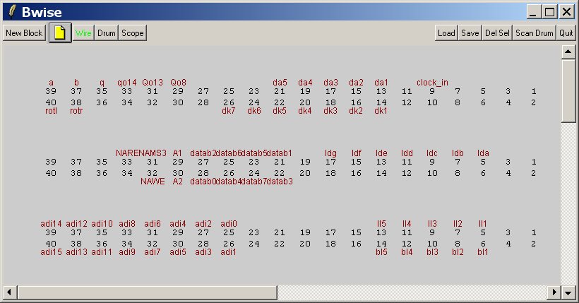
though with a bit small font in this version.
What are all these signals for? Well, mainly the Xilinx is used with a Analog Devices EZLITE Blackfin Digital Signal Processor board, to interface the DSP with the outside world. The upper left signals are for interfacing a rotary knob (rotate left/right) abd some divided clock signals (with low frequency based on the onboard crystal). Then the upper row contains in the middle the signals to drive a 5x7 LED display (see Using BWise 7x5 segment block to program a DSP/Xilinx driven display), and the crystal clock signal.
The middle row (connector B I think) has on the left the NotAsynchronousReadEnable and write enable bus signals from the DSP, and the AsynchronousMemorySelect bank 3 signal, which maps a small memory space from the DSP to talk with the Xilinx, and in the middle in connector order the lower 8 data bus bits. On the right, 7 segment LED display outputs, for a hexadecimal readout of the rotary know counter (which works on the Xilinx, not needing the DSP).
The third connector shows 16 inputs on the left which are from a very fast (2 megasample per second) AD converter chip I'm trying out as a sample, which can be read by the dsp or shown as bits on the display with realtime feedback, and on the right there's a block of pins dedicated to 5 debounced switches with LED feedback.
The setup is quickly presented after I spent a few hours dealing with this problem, it needs a bit of work to make it into a full fledged tool which can be automatically reused when the xilinx design changes, for instance the text widget would better be replace by direct file IO, but this problem isn't time critical.