A simple BWise to VHDL example
It is trivial to make the comparison between Bwise and its blocks and connections and hardware design as can be done with Verilog or VHDL, for which there are major EE and other types of groups of people where Tcl is used quite a bit, for general scripting, like in the Xilinx Webpack IDE I use (see e.g. VHDL and Tcl).
In this case, which should be easy to recognize for people with experience in the field, I take this design to make a bwise equivalent of (which should be understandable for people with basic computer knowledge):
 library IEEE;
 use IEEE.STD_LOGIC_1164.ALL;
 use IEEE.STD_LOGIC_ARITH.ALL;
 use IEEE.STD_LOGIC_UNSIGNED.ALL;

 entity logicblock is
   Port ( i : in std_logic_vector(1 downto 0);
               o : out std_logic_vector(1 downto 0));
 end logicblock;

 architecture logicblock_arc of logicblock is
 begin
   o <= i(1) & (i(1) and i(0));
 end logicblock_arc;

 library IEEE;
 use IEEE.STD_LOGIC_1164.ALL;
 use IEEE.STD_LOGIC_ARITH.ALL;
 use IEEE.STD_LOGIC_UNSIGNED.ALL;

 entity top is
    Port ( BTN_EAST : in  STD_LOGIC;
           BTN_NORTH : in  STD_LOGIC;
           BTN_SOUTH : in  STD_LOGIC;
           BTN_WEST : in  STD_LOGIC;
           SW : in  STD_LOGIC_VECTOR (3 downto 0);
           LED : out  STD_LOGIC_VECTOR (7 downto 0));
 end top;


 architecture Behavioral of top is

 component logicblock is
   Port ( i : in std_logic_vector(1 downto 0);
               o : out std_logic_vector(1 downto 0));
 end component;

 begin

 -- LED(0) <= SW(0);
 -- LED(1) <= SW(3);

 -- a fixed bit pattern for some LEDs
 LED(7 downto 2) <= "101010";

 -- the two lower LEDs respond to switches
 -- with a logic function to determine how:
 logic1: logicblock port map (SW(1 downto 0),LED(1 downto 0));

 end Behavioral;
This time, I won't use the schematic editor of the Xilinx software to make the top level diagram, though I throw in the netlist for people who want to try it out for themselves to play with this all, which is for a Digilent Spartan 3E starter kit board, and for the Xilinx webpack, but it shouldn´t be too hard to adapt to other envs and boards:
 NET "BTN_EAST" LOC = "H13" | IOSTANDARD = LVTTL | PULLDOWN ;
 NET "BTN_NORTH" LOC = "V4" | IOSTANDARD = LVTTL | PULLDOWN ;
 NET "BTN_SOUTH" LOC = "K17" | IOSTANDARD = LVTTL | PULLDOWN ;
 NET "BTN_WEST" LOC = "D18" | IOSTANDARD = LVTTL | PULLDOWN ;

 NET "SW<0>" LOC = "L13" | IOSTANDARD = LVTTL | PULLUP ;
 NET "SW<1>" LOC = "L14" | IOSTANDARD = LVTTL | PULLUP ;
 NET "SW<2>" LOC = "H18" | IOSTANDARD = LVTTL | PULLUP ;
 NET "SW<3>" LOC = "N17" | IOSTANDARD = LVTTL | PULLUP ;

 NET "LED<7>" LOC = "F9" | IOSTANDARD = LVTTL | SLEW = SLOW | DRIVE = 8 ;
 NET "LED<6>" LOC = "E9" | IOSTANDARD = LVTTL | SLEW = SLOW | DRIVE = 8 ;
 NET "LED<5>" LOC = "D11" | IOSTANDARD = LVTTL | SLEW = SLOW | DRIVE = 8 ;
 NET "LED<4>" LOC = "C11" | IOSTANDARD = LVTTL | SLEW = SLOW | DRIVE = 8 ;
 NET "LED<3>" LOC = "F11" | IOSTANDARD = LVTTL | SLEW = SLOW | DRIVE = 8 ;
 NET "LED<2>" LOC = "E11" | IOSTANDARD = LVTTL | SLEW = SLOW | DRIVE = 8 ;
 NET "LED<1>" LOC = "E12" | IOSTANDARD = LVTTL | SLEW = SLOW | DRIVE = 8 ;
 NET "LED<0>" LOC = "F12" | IOSTANDARD = LVTTL | SLEW = SLOW | DRIVE = 8 ;
This file defines the external connections, in this case to the mentioned board, of which for this first example only two switches and 8 leds are used.
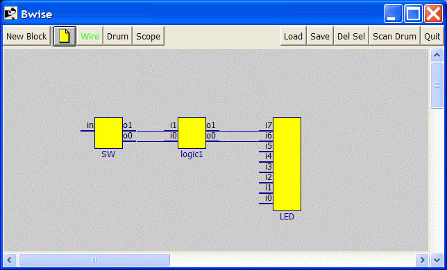
Schematically in Bwise:
which can be made for instance like this (from the bwise console):
 eval [pro_args newproc {{name {LED}}  {in {i7 i6 i5 i4 i3 i2 i1 i0}}  {out {}}}]
 eval [pro_args newproc {{name {SW}}  {out {o1 o0}}}]
 eval [pro_args newproc {{name {logic1}}   {in {i1 i0}}  {out {o1 o0}}}]
and then dragging the blocks in place and putting connections in between.
To do this automatic, we want to simplify the bus connections and possibly make named connection wires instead of using the map with IO identifiers.
See also Bwise, a serial port tcl script and a Xilinx demo board for various attempts to drive logic with tcl and bwise.
